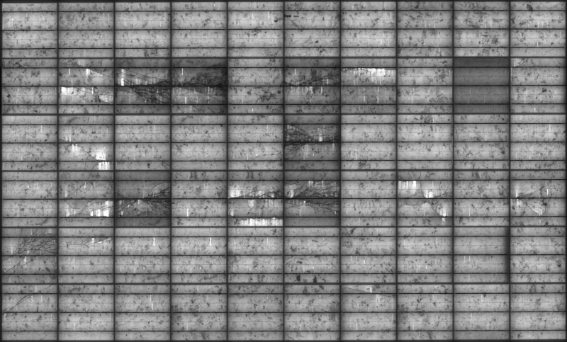
Line Scan PL-Imaging

Inspection of crystalline silicon photovoltaic modules using line scan luminescence imaging.
This work demonstrates luminescence imaging employed using a line scan methodology for the inspection of crystalline silicon PV modules. Experimental work has focused on identification of module faults, determination of quantitative performance metrics, and degradation monitoring. Contrary to conventional area scan imaging, line scan imaging restricts the camera field of view to a narrow line spanning the width of a module, which greatly simplifies acquisition for large area commercial modules. Two different techniques are explored using a prototype imaging tool developed at UNSW Sydney: line scan electroluminescence (ELLS) and photoluminescence (PLLS) imaging. Both provide comparable information; however, each has its own advantages and shortcomings.
The prototype imaging tool can acquire ELLS and PLLS images of full area industrial modules up to 72 cells [1], with inspection speeds of up to 0.2 m/s having been demonstrated. Each cell within a full area module can be imaged with a maximum resolution of 1120 square pixels, allowing for very fine features such as micro-cracks to be readily identified. Commercialisation of this tool is currently being undertaken by BT Imaging Pty Ltd.
Funded by Australian Renewable Energy Agency (ARENA) grant RND009.
Related publications:
[1] I. Zafirovska, M. K. Juhl, J. W. Weber, O. Kunz, and T. Trupke, "Module Inspection Using Line Scanning Photoluminescence Imaging," in 32nd European Photovoltaic Solar Energy Conference and Exhibition (32nd EU PVSEC), Munich, Germany, 2016, pp. 1826-1829.
[2] I. Zafirovska, M. K. Juhl, and T. Trupke, "Efficient Detection of Finger Interruptions from Photoluminescence Images," in 33rd European Photovoltaic Solar Energy Conference and Exhibition (33rd EU PVSEC), Amsterdam, The Netherlands, 2017, pp. 1689-1693.
[3] I. Zafirovska, M. K. Juhl, J. W. Weber, J. Wong, and T. Trupke, "Detection of Finger Interruptions in Silicon Solar Cells Using Line Scan Photoluminescence Imaging," IEEE Journal of Photovoltaics, vol. 7, pp. 1496-1502, November 2017.
[4] I. Zafirovska, M. K. Juhl, and T. Trupke, "Comparison of Line Scan Luminescence Imaging Techniques for Defect Characterisation in Crystalline Silicon Solar Modules," in 7th World Conference on Photovoltaic Energy Conversion (WCPEC-7), Waikoloa, Hawaii, USA, 2018.

